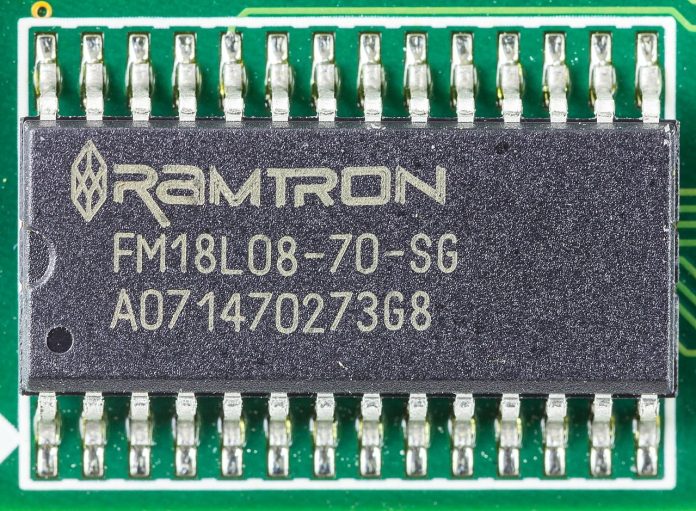
Engineers have developed a way that the millions of transistors used to process information could also store information.
The method, detailed in a paper published in Nature Electronics, accomplishes this by solving another problem: combining a transistor with higher-performing memory technology than is used in most computers, called ferroelectric RAM.
Researchers have been trying for decades to integrate the 2, but issues happen at the interface between a ferroelectric material and silicon, the semiconductor material that makes up transistors. Instead, ferroelectric RAM operates as a separate unit on-chip, limiting its potential to make computing much more efficient.
A team led by Peide Ye, the Richard J. and Mary Jo Schwartz Professor of Electrical and Computer Engineering at Purdue University, discovered how to integrate silicon and a ferroelectric material.
“We used a semiconductor that has ferroelectric properties,” Peide Ye said. “This way 2 materials become one material, and you don’t have to worry about the interface issues,” Ye said.
The result is a so-called ferroelectric semiconductor field-effect transistor, built in the same way as transistors currently used on computer chips.
The material, alpha indium selenide, not only has ferroelectric properties, but also addresses the issue of a conventional ferroelectric material usually acting as an insulator rather than a semiconductor due to a so-called wide band gap, which means that electricity cannot pass through and no computing happens.
In the past, researchers hadn’t been able to build a high-performance ferroelectric tunneling junction because its wide band gap made the material too thick for electrical current to pass through. Since alpha indium selenide has a much smaller band gap, the material can be just 10 nanometers thick without losing ferroelectric properties, allowing more current to flow through it.
More current allows a device area to scale down to several nanometers, making chips denser and energy efficient, Ye said. A thinner material — even down to an atomic layer thick – also means that the electrodes on either side of a tunnelling junction can be much smaller, which would be useful for building circuits that mimic networks in the human brain.
#sen.news


