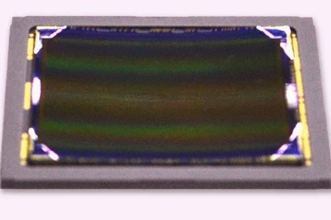
SONY engineers have created curved CMOS sensors, which according to Kazuichiro Itonaga, device manager with Sony's R&D Platform in Atsugi-shi, Japan, mean 50 per cent greater sensitivity in low light and simpler lenses.
Sony told the Symposium on VLSI Technology in Honolulu, Hawaii, that the curved systems were 1.4 times more sensitive at the centre of the sensor and twice as sensitive at the edge. This should mean the sensors offer improvements in low light performance of at least 50 per cent over current devices.
Itonga showed delegates 2 chips – one was 43 millimeters along the diagonal and is a full-size chip for digital cameras, including CCTV cameras. The other is smaller at 11mm diagonal, has smaller pixels and is designed for mobile phones.
The idea behind the curved CMOS is that it will remove many of the challenges faced by engineers trying to design out Petzval curvature of camera imaging systems. Petzval curvature is caused because lenses image a flat plane onto a flat CMOS sensor.
The issue is that there’s an attenuation of focal length light rays sensed by a CMOS imager if those light rays are off-axis – if they are reaching the imager from an oblique angle – the greater the angle, the greater the attenuation.
Quality lens designer put a lot of work into resolving field curvature using lens systems with field flattening capabilities but this process increases lens complexity, cost and weight. The process of resolving field curvature also causes problems – primarily astigmatism.
According to Itonga, the curved chips can be paired with a flatter lenses with larger apertures – that means more light reaches the sensors. It also means light rays get to the sensor in straighter lines, improving overall CMOS performance.
Something cool is that the process of bending the CMOS sensors had a surprising effect. When you bending a silicon sensor you alter its band gap and this lowers the noise level caused by dark current — which is the current that moves through a pixel in darkness.
Itonaga said a special machine was used to bend the CMOS sensors, which were backed with a ceramic to stabilize them. Itonaga said that the bend in the chips achieved the same level of curvature found in the human eye.
Once the bending process was complete, the engineers integrated the curved image sensor with a lensing system. Reports from the Symposium said while the Sony team showed delegates images from the new camera, they didn’t show them alongside existing technology for comparison.


